AD6620 part1 - Apuntes 1 PDF

| Title | AD6620 part1 - Apuntes 1 |
|---|---|
| Course | Circuitos Eléctricos |
| Institution | Universidad Alas Peruanas |
| Pages | 5 |
| File Size | 213.3 KB |
| File Type | |
| Total Downloads | 54 |
| Total Views | 141 |
Summary
Circuitos procesador 1...
Description
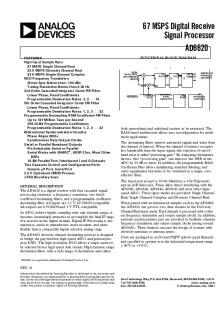
67 MSPS Digital Receive Signal Processor AD6620
a FEATURES High Input Sample Rate 67 MSPS Single Channel Real 33.5 MSPS Diversity Channel Real 33.5 MSPS Single Channel Complex NCO Frequency Translation Worst Spur Better than –100 dBc Tuning Resolution Better than 0.02 Hz 2nd Order Cascaded Integrator Comb FIR Filter Linear Phase, Fixed Coefficients Programmable Decimation Rates: 2, 3 . . . 16 5th Order Cascaded Integrator Comb FIR Filter Linear Phase, Fixed Coefficients Programmable Decimation Rates: 1, 2, 3 . . . 32 Programmable Decimating RAM Coefficient FIR Filter Up to 134 Million Taps per Second 256 20-Bit Programmable Coefficients Programmable Decimation Rates: 1, 2, 3 . . . 32 Bidirectional Synchronization Circuitry Phase Aligns NCOs Synchronizes Data Output Clocks Serial or Parallel Baseband Outputs Pin Selectable Serial or Parallel Serial Works with SHARC® , ADSP-21xx, Most Other DSPs 16-Bit Parallel Port, Interleaved I and Q Outputs Two Separate Control and Configuration Ports Generic P Port, Serial Port 3.3 V Optimized CMOS Process JTAG Boundary Scan GENERAL DESCRIPTION
The AD6620 is a digital receiver with four cascaded signalprocessing elements: a frequency translator, two fixedcoefficient decimating filters, and a programmable coefficient decimating filter. All inputs are 3.3 V LVCMOS compatible. All outputs are LVCMOS and 5 V TTL compatible. As ADCs achieve higher sampling rates and dynamic range, it becomes increasingly attractive to accomplish the final IF stage of a receiver in the digital domain. Digital IF Processing is less expensive, easier to manufacture, more accurate, and more flexible than a comparable highly selective analog stage. The AD6620 diversity channel decimating receiver is designed to bridge the gap between high-speed ADCs and general purpose DSPs. The high resolution NCO allows a single carrier to be selected from a high speed data stream. High dynamic range decimation filters with a wide range of decimation rates allow
FUNCTIONAL BLOCK DIAGRAM I REAL, DUAL REAL, OR COMPLEX INPUTS
Q
COS
AD6620
I CIC FILTERS
Q
I FIR FILTER
Q
OUTPUT FORMAT
SERIAL OR PARALLEL OUTPUTS
–SIN
COMPLEX NCO
EXTERNAL SYNC CIRCUITRY
JTAG PORT
P OR SERIAL CONTROL
both narrowband and wideband carriers to be extracted. The RAM-based architecture allows easy reconfiguration for multimode applications. The decimating filters remove unwanted signals and noise from the channel of interest. When the channel of interest occupies less bandwidth than the input signal, this rejection of out-ofband noise is called “processing gain.” By using large decimation factors, this “processing gain” can improve the SNR of the ADC by 36 dB or more. In addition, the programmable RAM Coefficient filter allows antialiasing, matched filtering, and static equalization functions to be combined in a single, costeffective filter. The input port accepts a 16-bit Mantissa, a 3-bit Exponent, and an A/B Select pin. These allow direct interfacing with the AD6600, AD6640, AD6644, AD9042 and most other highspeed ADCs. Three input modes are provided: Single Channel Real, Single Channel Complex, and Diversity Channel Real. When paired with an interleaved sampler such as the AD6600, the AD6620 can process two data streams in the Diversity Channel Real input mode. Each channel is processed with coherent frequency translation and output sample clocks. In addition, external synchronization pins are provided to facilitate coherent frequency translation and output sample clocks among several AD6620s. These features can ease the design of systems with diversity antennas or antenna arrays. Units are packaged in an 80-lead PQFP (plastic quad flatpack) and specified to operate over the industrial temperature range (–40°C to +85°C).
SHARC is a registered trademark of Analog Devices, Inc.
REV. A Information furnished by Analog Devices is believed to be accurate and reliable. However, no responsibility is assumed by Analog Devices for its use, nor for any infringements of patents or other rights of third parties that may result from its use. No license is granted by implication or otherwise under any patent or patent rights of Analog Devices.
One Technology Way, P.O. Box 9106, Norwood, MA 02062-9106, U.S.A. Tel: 781/329-4700 www.analog.com Fax: 781/326-8703 © Analog Devices, Inc., 2001
AD6620 TABLE OF CONTENTS
ARCHITECTURE
GENERAL DESCRIPTION . . . . . . . . . . . . . . . . . . . . . . . . . 1
As shown in Figure 1, the AD6620 has four main signal processing stages: a Frequency Translator, two Cascaded Integrator Comb FIR Filters (CIC2, CIC5), and a RAM Coefficient FIR Filter (RCF). Multiple modes are supported for clocking data into and out of the chip. Programming and control is accomplished via serial and microprocessor interfaces.
ARCHITECTURE . . . . . . . . . . . . . . . . . . . . . . . . . . . . . . . . 2 SPECIFICATIONS . . . . . . . . . . . . . . . . . . . . . . . . . . . . . . . 4 TIMING . . . . . . . . . . . . . . . . . . . . . . . . . . . . . . . . . . . . . . . . 5 ABSOLUTE MAXIMUM RATINGS . . . . . . . . . . . . . . . . 11 EXPLANATION OF TEST LEVELS . . . . . . . . . . . . . . . . 11 ORDERING GUIDE . . . . . . . . . . . . . . . . . . . . . . . . . . . . . 11 PIN FUNCTION DESCRIPTIONS . . . . . . . . . . . . . . . . . 12 PIN CONFIGURATIONS . . . . . . . . . . . . . . . . . . . . . . . . . 13 INPUT DATA PORT . . . . . . . . . . . . . . . . . . . . . . . . . . . . . 15 OUTPUT DATA PORT . . . . . . . . . . . . . . . . . . . . . . . . . . . 18 FREQUENCY TRANSLATOR . . . . . . . . . . . . . . . . . . . . . 19 SECOND ORDER CASCADED INTEGRATOR COMB FILTER . . . . . . . . . . . . . . . . . . . . . . . . . . . . . . . 21 FIFTH ORDER CASCADED INTEGRATOR COMB FILTER . . . . . . . . . . . . . . . . . . . . . . . . . . . . . . . 23 RAM COEFFICIENT FILTER . . . . . . . . . . . . . . . . . . . . . 25 CONTROL REGISTERS AND ON-CHIP RAM . . . . . . . 27 PROGRAMMING THE AD6620 . . . . . . . . . . . . . . . . . . . 30 ACCESS PROTOCOLS . . . . . . . . . . . . . . . . . . . . . . . . . . . 31 MICROPORT CONTROL . . . . . . . . . . . . . . . . . . . . . . . . 32 SERIAL PORT CONTROL . . . . . . . . . . . . . . . . . . . . . . . . 35 JTAG BOUNDARY SCAN . . . . . . . . . . . . . . . . . . . . . . . . 37 APPLICATIONS . . . . . . . . . . . . . . . . . . . . . . . . . . . . . . . . 38
Input data to the chip may be real or complex. If the input data is real, it may be clocked in as a single channel or interleaved with a second channel. The two-channel input mode, called Diversity Channel Real, is typically used in diversity receiver applications. Input data is clocked in 16-bit parallel words, IN[15:0]. This word may be combined with exponent input bits EXP[2:0] when the AD6620 is being driven by floating-point or gain-ranging analog-to-digital converters such as the AD6600. Frequency translation is accomplished with a 32-bit complex Numerically Controlled Oscillator (NCO). Real data entering this stage is separated into in-phase (I) and quadrature (Q) components. This stage translates the input signal from a digital intermediate frequency (IF) to baseband. Phase and amplitude dither may be enabled on-chip to improve spurious performance of the NCO. A phase offset word is available to create a known phase relationship between multiple AD6620s. Following frequency translation is a fixed coefficient, high speed decimating filter that reduces the sample rate by a programmable ratio between 2 and 16. This is a second order, cascaded integrator comb FIR filter shown as CIC2 in Figure 1. (Note: Decimation of 1 in CIC2 requires 2× or greater clock into AD6620). The data rate into this stage equals the input data rate, fSAMP. The data rate out of CIC2, fSAMP2, is determined by the decimation factor, MCIC2.
OUTLINE DIMENSIONS . . . . . . . . . . . . . . . . . . . . . . . . . 44 RCF 3
EXP[2:0] IN[15:0]
I-RAM 256 ⴛ 18
16
INTERLEAVE
INPUT DATA
DEINTERLEAVE CIC5
SCALING
FREQUENCY 3 TRANSLATOR I 18 16 Q 18
CIC2 EXP SCALING
MULTIPLEXER
f SAMP5
PHASE OFFSET CLK A/B
TIMING
RESET
SYNC NCO SYNC CIC
Q-RAM 256 ⴛ 18
23 23
M CICS
OUTPUT
f SAMP2 COMPLEX NCO
RCF COEFFICIENTS NUMBER OF TAPS DECIMATE FACTOR CIC2, CIC5 DECIMATE FACTORS ADDRESS OFFSET f SAMP SCALE FACTORS OUTPUT NCO FREQUENCY SCALE PHASE OFFSET FACTOR DITHER SYNC MASK CONTROL REGISTERS INPUT MODE MICROPORT AND REAL, DUAL, COMPLEX SERIAL ACCESS FIXED OR WITH EXPONENT SYNC M/S
I/QOUT MULTIPLEXER
PARALLEL
MICROPROCESSOR INTERFACE
JTAG
SYNC RCF TRST
TCK TMS
TDI
TDO
D[7:0] A[2:0] CS
DVOUT
SCALING, SOUT
EXPLNV, EXPOFF
SYNC I/O
M RCF
M CICS
MULTIPLEXER
SCALING
C-RAM 256 ⴛ 20
R/W
DS
(W/R) (R/D)
DTACK (RDY)
MODE PAR/SER
A/BOUT
SERIAL
16
PARALLEL OUTPUTS AND SERIAL I/O
16
OUT[15:0] SCLK SDI SDO SDFS SDFE SBM WL[1:0] AD SDIV[3:0]
Figure 1. Block Diagram
–2–
REV. A
AD6620 The overall filter response for the AD6620 is the composite of all three cascaded decimating filters: CIC2, CIC5, and RCF. Each successive filter stage is capable of narrower transition bandwidths but requires a greater number of CLK cycles to calculate the output. More decimation in the first filter stage will minimize overall power consumption. Data comes out via a parallel port or a serial interface.
Following CIC2 is the second fixed-coefficient decimating filter. This filter, CIC5, further reduces the sample rate by a programmable ratio from 1 to 32. The data rate out of CIC5, fSAMP5, is determined by the decimation factors of MCIC5 and MCIC2. Each CIC stage is a FIR filter whose response is defined by the decimation rate. The purpose of these filters is to reduce the data rate of the incoming signal so that the final filter stage, a FIR RAM coefficient sum-of-products filter (RCF), can calculate more taps per output. As shown in Figure 1, on-chip multiplexers allow both CIC filters to be bypassed if a multirate clock is used.
Figure 2 illustrates the basic function of the AD6620: to select and filter a single channel from a wide input spectrum. The frequency translator “tunes” the desired carrier to baseband. CIC2 and CIC5 have fixed order responses; the RCF filter provides the sharp transitions. More detail is provided in later sections of the data sheet.
The fourth stage is a sum-of-products FIR filter with programmable 20-bit coefficients, and decimation rates programmable from 1 to 32. The RAM Coefficient FIR Filter (RCF in Figure 1) can handle a maximum of 256 taps.
(–fsamp/2 TO fsamp/ 2)
WIDEBAND INPUT SPECTRUM C'
SIGNAL OF INTEREST "IMAGE"
D'
–f S /2
A
A'
B
B'
–3f S/8
–5fS /16
–f S /4
–3fS /16
–f S/8
–f S /16
fS /16
DC
fS/8
3f S /16
SIGNAL OF INTEREST
C D
f S/4
5fS /16
3fS /8
fS /2
Figure 2a. Wideband Input Spectrum (e.g., 30 MHz from High-Speed ADC) NCO "TUNES" SIGNAL TO BASEBAND AFTER FREQUENCY TRANSLATION A
–f S /2
–3fS /8
–5f S/16
–f S /4
–3f S/16
C'
C
B
D
–f S /8
–f S /16
DC
fS /16
A'
B'
D'
fS/8
3f S/16
fS /4
5f S /16
3f S /8
Figure 2b. Frequency Translation (e.g., Single 1 MHz Channel Tuned to Baseband)
CIC2, CIC5, AND RCF 0 –10 –20 –30 –40
dBc
–50 –60 –70 –80 –90 –100 –110 –120 –130 FREQUENCY
Figure 2c. Baseband Signal is Decimated and Filtered by CIC2, CIC5, RCF
REV. A
–3–
fS/2
AD6620–SPECIFICATIONS
RECOMMENDED OPERATING CONDITIONS Parameter
Test Level
Min
AD6620AS Typ
Max
Unit
VDD TAMBIENT
I IV
3.0 –40
3.3 +25
3.6 +85
V °C
Temp
Test Level
Min
AD6620AS Typ
Max
Unit
Full Full Full Full Full 25°C
I I I I V
2.0 –0.3
VDD + 0.3 0.8 10 10
V V µA µA pF
LOGIC OUTPUTS2, 4, 7, 8, 9, 10, 11 Logic Compatibility Logic “1” Voltage (IOH = 0.5 mA) Logic “0” Voltage (IOL = 1.0 mA)
Full Full Full
I I
2.4
IDD SUPPLY CURRENT CLK = 20 MHz12 CLK = 65 MHz13 Reset Mode14
Full Full Full
V I I
52 167
POWER DISSIPATION CLK = 20 MHz12 CLK = 65 MHz13 Reset Mode14
Full Full Full
V I I
170 550
ELECTRICAL CHARACTERISTICS Parameter (Conditions) 1, 2, 3, 4, 5, 6, 7
LOGIC INPUTS Logic Compatibility Logic “1” Voltage Logic “0” Voltage Logic “1” Current Logic “0” Current Input Capacitance
(NOT 5 V TOLERANT) 3.3 V CMOS
1 1 4
3.3 V CMOS/TTL VDD – 0.2 0.2 0.4
V V
227 1
mA mA mA
750 3.3
mW mW mW
NOTES 1Input-Only Pins: CLK, RESET, IN[15:0], EXP[2:0], A/B, PAR/SEL. 2 Bidirectional Pins: SYNC_NCO, SYNC_CIC, SYNC_RCF. 3Microinterface Input Pins: DS (RD ), R/W ( WR), CS. 4 Microinterface Bidirectional Pins: A[2:0], D[7:0]. 5JTAG Input Pins: TRST, TCK, TMS, TDI. 6 Serial Mode Input Pins: SDI, SBM, WL[1:0], AD, SDIV[3:0]. 7 Serial Mode Bidirectional Pins: SCLK, SDFS. 8 Output Pins: OUT[15:0], DVOUT, A/B OUT, I/Q OUT. 9Microinterface Output Pins: DTACK (RDY). 10 JTAG Output Pins: TDO. 11 Serial Mode Output Pins: SDO, SDFE. 12 Conditions for IDD @ 20 MHz. MCIC2 = 2, M CIC5 = 2, MRCF = 1, 4 RCF taps of alternating positive and negative full scale. 13 Conditions for IDD @ 65 MHz. MCIC2 = 2, M CIC5 = 2, MRCF = 1, 4 RCF taps of alternating positive and negative full scale. 14 Conditions for IDD in Reset ( RESET = 0). Specifications subject to change without notice.
–4–
REV. A
AD6620 TIMING CHARACTERISTICS (C
LOAD
= 40 pF All Outputs)
Parameter (Conditions)
Temp
Test Level
Min
CLK Timing t CLK t CLK t CLKL t CLKH
Full Full Full Full
I I IV IV
14.931 15.4 7.0 7.0
Reset Timing Requirements: RESET Width Low t RESL
Full
I
30.0
ns
Input Data Timing Requirements: t SI Input2 to CLK Setup Time t HI Input2 to CLK Hold Time
Full Full
IV IV
–1.0 6.5
ns ns
Parallel Output Switching Characteristics: CLK to OUT[15:0] Rise Delay t DPR CLK to OUT[15:0] Fall Delay t DPF t DPR CLK to DVOUT Rise Delay CLK to DVOUT Fall Delay t DPF t DPR CLK to IQOUT Rise Delay t DPF CLK to IQOUT Fall Delay CLK to ABOUT Rise Delay t DPR CLK to ABOUT Fall Delay t DPF
Full Full Full Full Full Full Full Full
IV IV IV IV IV IV IV IV
8.0 7.5 6.5 5.5 7.0 6.0 7.0 5.5
SYNC Timing Requirements: t SY SYNC3 to CLK Setup Time SYNC3 to CLK Hold Time t HY
Full Full
IV IV
–1.0 6.5
SYNC Switching Characteristics: t DY CLK to SYNC4 Delay Time
Full
V
7.0
Serial Input Timing: t SSI SDI to SCLKt Setup Time t HSI SDI to SCLKt Hold Time t HSRF SDFS to SCLKu Hold Time t SSF SDFS to SCLKt Setup Time5 t HSF SDFS to SCLKt Hold Time5
Full Full Full Full Full
IV IV IV IV IV
1.0 2.0 4.0 1.0 2.0
Serial Frame Output Timing: SCLKu to SDFE Delay Time t DSE t SDFEH SDFE Width High SCLKu to SDO Delay Time t DSO
Full Full Full
IV V IV
3.5
SCLK Switching Characteristics, SBM = “1”: SCLK Period4 t SCLK t SCLKL SCLK Width Low t SCLKH SCLK Width High CLK to SCLK Delay Time t SCLKD
Full Full Full Full
I V V V
2 × tCLK
Serial Frame Timing, SBM = “1”: t DSF SCLKu to SDFS Delay Time t SDFSH SDFS Width High
Full Full
IV V
1.0
SCLK Timing Requirements, SBM = “0”: SCLK Period t SCLK t SCLKL SCLK Width Low SCLK Width High t SCLKH
Full Full Full
I IV IV
15.4 0.4 × tSCLK 0.4 × tSCLK
Requirements: CLK Period CLK Period CLK Width Low CLK Width High
AD6620AS Typ
REV. A
–5–
Unit ns ns ns ns
0.5 × tCLK 0.5 × tCLK
19.5 19.5 19.0 11.5 19.5 13.5 19.5 13.5
ns ns ns ns ns ns ns ns ns ns
23.5
ns ns ns ns ns ns
11.0 11.0
ns ns ns
13.0
ns ns ns ns
tSCLK 4.5
0.5 × tSCLK 0.5 × tSCLK 6.5
tSCLK
4.0
ns ns
0.5 × t SCLK 0.5 × t SCLK
ns ns ns
NOTES 1 This specification valid for VDD >= 3.3 V. CLKL t and t CLKH still apply. 2 Specification pertains to: IN[15:0], EXP[2:0], A/B. 3 Specification pertains to: SYNC_NCO, SYNC_CIC, SYNC_RCF. 4 SCLK period will be ≥ 2 × tCLK when AD6620 is Serial Bus Master (SBM = 1) depending on the SDIV word. 5 SDFS setup and hold time must be met, even when configured as outputs, since internally the signal is sampled at the pad. Specifications subject to change without notice.
Max...
Similar Free PDFs
AD6620 part1 - Apuntes 1
- 5 Pages

Selfass-part1
- 4 Pages
Problems chap5-part1
- 2 Pages

T1 Bus Arinc 429 part1 - Apunts 1
- 17 Pages

Klimek blue part1 - Blue Book Part 1
- 64 Pages

Linguagem C avançada - Part1
- 20 Pages

Résumé cours opération part1
- 16 Pages

Schema §263 Part1
- 1 Pages

Experimental Psych Notes Part1
- 16 Pages

CSL-Tema1 Amplificadors part1
- 6 Pages

Buku robotika Part1
- 132 Pages

Studyplan part1 (9,10)
- 42 Pages

MG slides 2018 part1
- 234 Pages
Popular Institutions
- Tinajero National High School - Annex
- Politeknik Caltex Riau
- Yokohama City University
- SGT University
- University of Al-Qadisiyah
- Divine Word College of Vigan
- Techniek College Rotterdam
- Universidade de Santiago
- Universiti Teknologi MARA Cawangan Johor Kampus Pasir Gudang
- Poltekkes Kemenkes Yogyakarta
- Baguio City National High School
- Colegio san marcos
- preparatoria uno
- Centro de Bachillerato Tecnológico Industrial y de Servicios No. 107
- Dalian Maritime University
- Quang Trung Secondary School
- Colegio Tecnológico en Informática
- Corporación Regional de Educación Superior
- Grupo CEDVA
- Dar Al Uloom University
- Centro de Estudios Preuniversitarios de la Universidad Nacional de Ingeniería
- 上智大学
- Aakash International School, Nuna Majara
- San Felipe Neri Catholic School
- Kang Chiao International School - New Taipei City
- Misamis Occidental National High School
- Institución Educativa Escuela Normal Juan Ladrilleros
- Kolehiyo ng Pantukan
- Batanes State College
- Instituto Continental
- Sekolah Menengah Kejuruan Kesehatan Kaltara (Tarakan)
- Colegio de La Inmaculada Concepcion - Cebu


