Lab1 homework Ripple Carry Adder PDF

| Title | Lab1 homework Ripple Carry Adder |
|---|---|
| Author | Soundarya Krishnan |
| Course | Custumer Relatiunship Measurement |
| Institution | University of Europe for Applied Sciences |
| Pages | 5 |
| File Size | 240.7 KB |
| File Type | |
| Total Downloads | 67 |
| Total Views | 149 |
Summary
Consumer Management tutorial sheet...
Description
What is Ripple Carry Adder?
A ripple carry adder also known as “n-bit parallel adder” is a combinational logic circuit used for the purpose of adding two n-bit binary numbers and requires ‘n’ full adders in the circuit.
4-bit Ripple Carry Adder
4-bit ripple carry adder is used for the purpose of adding two 4-bit binary numbers in twos complement form.
In mathematics, any two 4-bit binary numbers A 3A2A1 A0 and B3B2 B1B0 will be added as-
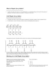
Using ripple carry adder, this addition will be carried out as shown by the following logic diagram-
As shown, Ripple Carry Adder works in different stages where the carry out produced by each full adder as output serves as the carry in input for its adjacent most significant full adder. When the carry in becomes available to the full adder, it activates that full adder and it comes into operation.
Working of a 4-bit Ripple Carry AdderSuppose we want to add two 4 bit binary numbers 0101 (A 3A2A1 A0) and 1010 (B 3B2B1 B0). Using ripple carry adder, this addition will be carried out as explained belowStage-01: When Cin will be fed as input to full Adder A, it will activate full adder A.
Then, At Full Adder A,
A0 = 1
B0 = 0
Cin = 0 The sum bit and carry bit produced as output by full adder A will be calculated by full adder A as-
Calculating S0 –
S0 = A 0 ⊕ B 0 ⊕ Cin
=1⊕0⊕0
C1 = 0 The sum bit and carry bit produced as output by full adder C will be calculated by full adder C as-
=1
Calculating S2 –
∴ S0 = 1
S 2 = A2 ⊕ B2 ⊕ C1
Calculating C0 –
=1⊕0⊕0
C0 = A 0B 0 ⊕ B 0Cin ⊕ C in A0
=1
= 1.0 ⊕ 0.0 ⊕ 0.1
∴ S2 = 1
=0⊕0⊕0
Calculating C2 –
=0
C 2 = A2 B2 ⊕ B 2C1 ⊕ C1A2
∴ C0 = 0
= 1.0 ⊕ 0.0 ⊕ 0.1
Stage-02:
=0⊕0⊕0
Now, when C o will be fed as input to full adder B by full adder A, it will activate full adder B.
=0
Then, At Full Adder B,
∴ C2 = 0
A1 = 0
C0 = 0
Stage-04: Now, when C 2 will be fed as input to full adder D by full adder C, it will activate full adder D.
B1 = 1
Then, At Full Adder D,
The sum bit and carry bit produced as output by full adder B will be calculated by full adder B as-
Calculating S1 – S1 = A 1 ⊕ B 1 ⊕ C0
A3 = 0
B3 = 1
C2 = 0 The sum bit and carry bit produced as output by full adder D will be calculated by full adder D as-
=0⊕1⊕0 =1
Calculating S3 –
∴ S1 = 1
S 3 = A3 ⊕ B3 ⊕ C2 = 0 ⊕ 1 ⊕ 0 = 1 ∴ S3 = 1
Calculating C1 –
Calculating C3 –
C1 = A 1B 1 ⊕ B1 C0 ⊕ C0A1
C 3 = A3 B3 ⊕ B3 C2 ⊕ C2A3
= 0.1 ⊕ 1.0 ⊕ 0.0
= 0.1 ⊕ 1.0 ⊕ 0.0
=0⊕0⊕0
=0⊕0⊕0
=0
=0
∴ C1 = 0
∴ C3 = 0
Stage-03: Now, when C 1 will be fed as input to full adder C by full adder B, it will activate full adder C. Then, At Full Adder C,
B2 = 0
A2 = 1
Thus finally,
Output Sum = S3 S2 S1 S0 = 1111 Output Carry = C3 = 0
Why Ripple Carry Adder is called so?
In Ripple Carry Adder, the carry out produced by each full adder as output serves as the carry in input for its next most significant full adder.
Since in ripple carry adder, each carry bit ripples or waves into the next stage, that’s why it is called by the name “Ripple Carry Adder”.
Limitation of Ripple Carry Adder
Ripple Carry Adder does not allow all full adders to be used simultaneously and each full adder has to necessarily wait till the carry bit becomes available from its adjacent less significant full adder.
This increases the propagation time and due to this reason, ripple carry adder becomes extremely slow which is considered to be the biggest disadvantage of using ripple carry adder.
Delay in Ripple Carry Adder
Carry propagation delay of a full adder is the time taken by it to produce the output carry bit.
Sum propagation delay of a full adder is the time taken by it to produce the output sum bit.
Worst case delay of a ripple carry adder is the time after which the output sum bit and carry bit becomes available from the last full adder.
Suppose we have a N-bit ripple carry adder as shown-
Type-01 Problem: You will be given the carry propagation delay and sum propagation delay of each full adder and you will be asked to calculate the worst case delay of the ripple carry adder.
Solution
We know, in ripple carry adder, a full adder becomes active only when its carry in is made available by its adjacent less significant full adder.
When carry in becomes available to the full adder, it starts its operation and produces the corresponding output sum bit and carry bit.
If you are asked to calculate the time after which the output sum bit or carry bit becomes available from any particular full adder, then you can calculate it asTime after which carry bit C x becomes available-
Required time = Total number of full adders till full adder producing C x X Carry propagation delay of a full adder Time after which sum bit S x becomes available-
Required time = Time taken for its carry in to become available + Sum propagation delay of a full adder = { Total number of full adders before full adder producing S x X Carry propagation delay of a full adder } + Sum propagation delay of a full adder NOTE-
We will calculate the worst case delay for the last full adder.
Type-02 Problem: You will be given the propagation delay of basic logic gates and you will be told how the full adder has been implemented and then you will be asked to calculate the worst case delay of ripple carry adder. Suppose each full adder in ripple carry adder is implemented as-
SolutionWe have to compute everything in the same manner as we did in the type-01 problem. It’s just that in Type-02 problem, one step is increased. We will first calculate the carry propagation delay and sum propagation delay in terms of propagation delays of basic logic gates and then our problem will be reduced to Type-01 problem. Let
Propagation delay of AND gate = T pd (AND)
Propagation delay of OR gate = T pd (OR)
Propagation delay of XOR gate = T pd (XOR) Calculating carry propagation delay-
We will calculate the carry propagation delay of a full adder using its carry generator logic circuit which in the given implementation has 2 levels.
At the first level, three AND gates operate. Because all the three AND gates operate in parallel, so we will consider the propagation delay due to only one AND gate and not because of all the three AND gates. At the second level, OR gate operates. Now, Carry propagation delay of a full adder which is the time taken by it to generate the output carry bit is given byCarry propagation delay = Propagation delay of AND gate + Propagation delay of OR gate = T pd (AND) + T pd (OR) Calculating sum propagation delay-
We will calculate the sum propagation delay of a full adder using its sum generator logic circuit which in the given implementation has only 1 level at which the XOR gate operates. Now, Sum propagation delay of a full adder which is the time taken by it to generate the output sum bit is given bySum propagation delay = Propagation delay of XOR gate = T pd (XOR) Now, after we have got the carry propagation delay and sum propagation delay of full adders, our problem reduces to Type-01 problem. Now, we will use the same formulas we have learnt in Type-01 problem to make the required calculations.
NOTE-
If in the question, it was said that while implementing the sum generator logic circuit of full adders, only 2input XOR gates are used, then in that case we would require two such XOR gates which would work at 2 levels. So, in that case, sum propagation delay would be twice the propagation delay of XOR gate....
Similar Free PDFs

Lab1 homework Ripple Carry Adder
- 5 Pages

Carry-Lookahead Adder
- 12 Pages

Laporan Half Adder dan Full Adder
- 13 Pages

METRO Cash carry case
- 31 Pages

Lab1
- 1 Pages

Lab1
- 5 Pages

Lab1
- 8 Pages

Emerging market carry trade
- 3 Pages

LAB1 - Matlab
- 5 Pages

Matlab Lab1
- 17 Pages

Lab1 - Lab
- 9 Pages

rangkaian adder dengan seven segment
- 26 Pages

Lab1 termo
- 15 Pages

Penny-Lab1
- 6 Pages
Popular Institutions
- Tinajero National High School - Annex
- Politeknik Caltex Riau
- Yokohama City University
- SGT University
- University of Al-Qadisiyah
- Divine Word College of Vigan
- Techniek College Rotterdam
- Universidade de Santiago
- Universiti Teknologi MARA Cawangan Johor Kampus Pasir Gudang
- Poltekkes Kemenkes Yogyakarta
- Baguio City National High School
- Colegio san marcos
- preparatoria uno
- Centro de Bachillerato Tecnológico Industrial y de Servicios No. 107
- Dalian Maritime University
- Quang Trung Secondary School
- Colegio Tecnológico en Informática
- Corporación Regional de Educación Superior
- Grupo CEDVA
- Dar Al Uloom University
- Centro de Estudios Preuniversitarios de la Universidad Nacional de Ingeniería
- 上智大学
- Aakash International School, Nuna Majara
- San Felipe Neri Catholic School
- Kang Chiao International School - New Taipei City
- Misamis Occidental National High School
- Institución Educativa Escuela Normal Juan Ladrilleros
- Kolehiyo ng Pantukan
- Batanes State College
- Instituto Continental
- Sekolah Menengah Kejuruan Kesehatan Kaltara (Tarakan)
- Colegio de La Inmaculada Concepcion - Cebu

